
Built to Lead.
Engineered to Last.
Wafer Prober
8” & 12” Wafer Prober
Introducing our our state-of-the-art 8″ and 12″ wafer probers, setting the benchmark for precision and performance in semiconductor testing. Built on a robust solid granite base for unparalleled stability. OS6000 boast a sophisticated linear motor system that ensures swift and highly accurate positioning. The introduction of MicroTouch (soft touchdown) technology guarantees delicate yet precise wafer handling ensures delicate handling of wafers, safeguarding against potential damage.
The closed-loop system, coupled with our proprietary Active Vibration Control (AVC), a feature that mitigates any disturbances and vibration (external or internal), maintaining an utmost optimal testing environment. What sets our probers apart are the unique software features that elevate performance to new heights, offering intuitive control and unmatched flexibility. With a focus on innovation and reliability, our wafer probers redefine precision in semiconductor testing.

Specifications Overview

Vision Inspection
Post Seal Vision Inspection Handler Series
The osRRS series is designed with advanced key technologies to provide for Reel-to-Reel Inspection.

osRRS
(Single Camera)

osRRSe
(Dual Camera)
Specifications Overview


Tray-based Vision Handler
Introducing Ocas Superior Tray-based Vision Handler which performs final inspection on various IC packages handled in tray.
Tray to Tray Series

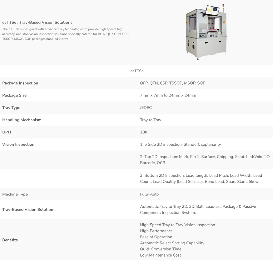
osTTSe

osSTS
Specifications Overview

Wafer Based Vision Machine
osWIS 100: Wafer Vision Inspection Machine
osWIS 100 Wafer Vision Inspection Handler offers advanced solution for 2D surface defect inspections, measurements and multiple handling mechanisms to support different wafer forms including raw wafer, hoop ring, and framed wafer range from 120mm (6”) to 300mm (12”).

Specifications Overview
